Patent 5059955
Note: All mentions of "dot" have been replaced with "pixel" (DCC is now PCC).
United States Patent Number: 5059955
In an apparatus for producing video signals in which a memory storing color data is addressed with an address signal determined by video data to produce color data, an analog RGB signal producing circuit in which the color data read from the memory are converted to analog signals is provided so that a color image can be displayed on a video display or an exclusively used monitor means to which the color data are directly supplied. Further, a signal conversion circuit, a video color signal producing circuit, and a composite circuit are provided wherein a luminance signal and color difference signals are produced in accordance with the color data in the signal conversion circuit, and the luminance signal is converted to an analog luminance signal and color carriers are produced by modulating analog signals converted from the color difference signals with the color subcarriers in the video color signal producing circuit. In the composite circuit, the analog luminance signal, the color carriers, and a burst signal obtained in accordance with the color subcarriers are combined to produce a composite signal so that a color image can be displayed on a video display to which the composite signal is supplied through a receiving circuit of a television set.
The invention relates to an apparatus for producing video signals, and more particularly to an apparatus for producing video signals in which analog RGB signals and composite signals are produced selectively.
In one of conventional apparatus for producing video signals, analog signals having amplitudes of R(ed), G(reen) and B(lue) are produced to be supplied to an exclusively used monitor means. The apparatus for producing video signals comprises a VRAM for storing video data, a color table RAM for storing color data, and a digital to analog converter for converting digital color data to analog color data.
In the apparatus for producing video signals, video data for each picture element are read from the VRAM, and the color table RAM is then addressed in accordance with an address signal which is of video data read from the video data RAM so that color data are read therefrom. Then, the color data are converted in the digital to analog converter to analog RGB signals which are supplied to the exclusively used monitor means so that a color image is displayed on the exclusively used monitor means. Color data is written into the color table RAM in accordance with a transfer thereof from a CPU thereto during horizontal and vertical retrace times so that a predetermined color image can be displayed in accordance with the color data.
According to the conventional apparatus for producing video signals, however, a color image can not be displayed on a video display of a television set to which a composite signal is required to be supplied because analog RGB signals are only produced therein. Although a composite signal is produced in accordance with a calculation based on analog RGB signals, a circuit construction becomes complicated so that an integrating density can not be increased as expected. Further, a hue of the color image is different from that in a television set even if such a composite signal is obtained in the calculation. Still further, flicker is occurred on a display at boarder color region due to indeterminate data of the CPU and the color table RAM in a case where color data are read from the color table RAM during the aforementioned transfer from the CPU to the color table RAM.
Accordingly, it is an object of the invention to provide an apparatus for producing video signals in which analog RGB signals and a composite signal are produced selectively.
It is a further object of the invention to provide an apparatus for producing video signals in which flicker is prevented from being occurred on a display during a transfer of color data.
- storing RGB color data at addresses defined in accordance with video data.
- producing analog RGB signals in accordance with a digital to analog conversion of said RGB color data.
- producing a luminance signal and color difference signals in accordance with said RGB color data.
- converting said luminance signal to an analog luminance signal and for producing color carriers by modulating analog signals converted from said color difference signals in accordance with color subcarriers.
- producing a composite signal by combining said analog luminance signal, said color carriers and a burst signal obtained in accordance with one of said color subcarriers.
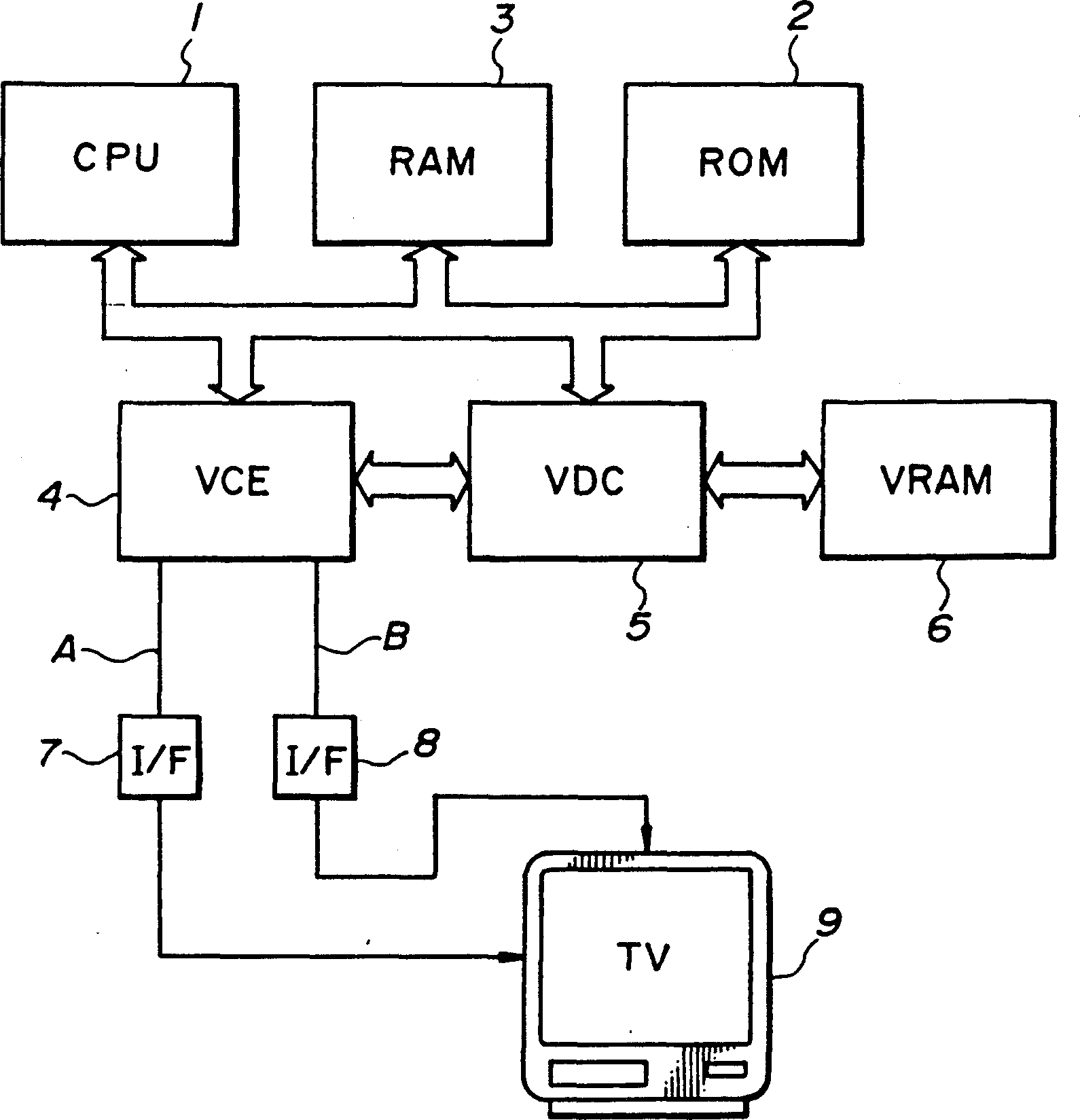
Figure 1: Block diagram of a color image displaying apparatus.
In [Figure 1], there is shown a color image displaying apparatus to which an apparatus for producing video signals is applied. The color image displaying apparatus comprises a CPU (1) for controlling the whole system, a ROM (2) for storing programs by which the whole system is controlled, a RAM (3) for storing data and calculation results temporarily, a Video Color Encoder (4) which is an apparatus for producing video signals in the invention and which produces output signals A of analog RGB signals and B of a composite signal, a Video Display Controller (5) for controlling a supply of video data to the Video Color Encoder (4), a VRAM (6) for storing video data to be supplied to the Video Color Encoder (4), and a video display (9) for displaying a color image in accordance with the analog RGB signals or the composite signal.

Figure 2: Block diagram of the Video Color Encoder.
[Figure 2] shows the Video Color Encoder (4) which is an apparatus for producing video signals in the embodiment according to the invention. In the Video Color Encoder (4), a 8/16 bit data bus interface (23) and an Address Register (24) are provided to be connected through a CPU data bus (21) of 9 bits D0 to D8 to the CPU (1), and an address selector (25) is provided to be connected through a VDC data bus (22) of 9 bits VD0 to VD8 to the Video Display Controller (5). The 8/16 bit data bus interface (23) has a function that the Video Color Encoder (4) is connected to the CPU (1) of 8 bits or 16 bits, and the address selector (25) selects one data from data in the Address Register (24) and data on the VDC data bus (22) as an address signal. A color table RAM (26) is connected to the 8/16 bit data bus interface (23), and a data latch circuit (27) having three outputs for R, G and B color data is connected to the color table RAM (26) so that color data read from the color table RAM (26) are latched in the data latch circuit (27). The three outputs of the data latch circuit (27) are connected to digital to analog converters (28, 29 and 30) for R, G and B color data and to a matrix ROM (31) having a signal conversion matrix therein in which color data are converted to a luminance signal Y, and color difference signals R-Y and B-Y. The 8/16 bit data bus interface (23), the Address Register (24), the address selector (25), the color table RAM (26), and the data latch circuit (27) are controlled together with a synchronous signal producing circuit (33) by a control circuit (32) having inputs of a 8/16 bit selection signal EX 8/16, a chip selection signal (CS), a writing signal (WR), a reading signal (RD), an output control signal (CESEL) etc. The synchronous signal producing circuit (33) receives an oscillation signal of a sinusoidal wave having a frequency of, for instance, 21.47727 MHz from an oscillation circuit (33A) and produces horizontal and vertical synchronous signals (HSYNC and VSYNC), pixel clock signals (CK), color subcarriers etc. The R, G and B digital to analog converters (28, 29 and 30) are connected to an analog RGB signal output circuit (41A) to which a synchronous signal composite circuit (34) is also connected. Outputs of the matrix ROM (31) are connected to digital to analog converters (35, 36 and 37) for the luminance signal Y, and the color difference signals R-Y and B-Y. The R-Y and B-Y digital to analog converters (36 and 37) are connected to modulators (38 and 39) in which the two color subcarriers of the same frequency and different phases by ninety degrees supplied from the synchronous signal producing circuit (33) are modulated by the color difference signals R-Y and B-Y, respectively, so that color carrier signals are produced therein. One of the color subcarriers is also supplied to a burst circuit (40) in which a burst signal is produced by inserting the color subcarrier of 8 or nine cycles at a period of back porch of the horizontal synchronous signal. In the Y digital to analog converter (35), the luminance signal is combined with the synchronous signals. The Y digital to analog converter (35), the modulators (38 and 39), and the burst circuit (40) are connected to a composite signal output circuit (41B).

Figure 3: Registers used in the Video Color Encoder.
In [Figure 3], there are explained a Control Register (CR), a Color Table Address register (CTA), a Color Table data Write register (CTW), and a Color Table data Read register (CTR) included in the control circuit (32). These registers are enabled with the chip selection signal (CS) 0 and one of them is selected with a content of the address A1 and A2 as follows.
In regard to a bit width selection, a bit width of 16 bits is selected when the signal EX 8/16 is 0, while a bit width of 8 bits is selected when the signal EX 8/16 is 1. In a case where the 8 bit width is selected, transferred data are of a lower byte for a register when the address A0 is 0, and transferred data are of an upper byte for a register when the address A0 is 1.
The Control Register (CR) includes frequency dividing data PCC in lower 8 bits.
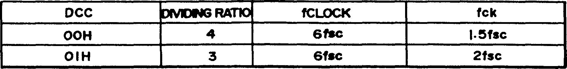
Figure 4: Frequency dividing ratio of the oscillation frequency.
In [Figure 4], there is explained a relation between an oscillation frequency of a sinusoidal wave in the oscillation circuit (31A) and a square wave pixel clock frequency (CK) wherein the dividing ratio is four when the content PCC is 0x00, and the dividing ratio is three when the content PCC is 0x01. In [Figure 4], the expression "fsc " indicates a frequency of a color subcarrier so that the expression "6fsc " means that a sinusoidal wave having a frequency of six times that of the color subcarrier is supplied to the synchronous signal producing circuit (33). Thus, the frequency dividing ratio of the synchronous signal producing circuit (33) is controlled by the Control Register (CR).
The Color Table Address register (CTA) includes a starting address CTA at lower 9 bits. The starting address is an address for the color table RAM (26) from which data transferred from the CPU (1) are started to be written into the color table RAM (26). When an address is set in the Address Register (24), the address is automatically incremented by one each time when data are read or written.
The Color Table data Write register (CTW) and the Color Table data Read register (CTR) include 3 bit color data for R, G and B at lower 9 bits respectively, and are used for a transfer of data between the CPU (1) and the color table RAM (26).

Figure 5: Explanation of video data.
[Figure 5] shows video data VD0 to VD8 supplied from the Video Display Controller (5). The most significant bit VD8 defines a kind of data, that is, when the bit VD8 is 0, the data VD0 to VD7 are of a background, and when the bit VD8 is 1, the data VD0 to VD7 are of a sprite. In the data VD0 to VD7, the upper 4 bits VD4 to VD7 are of an address signal for addressing area color (a designation of a block), and the lower 4 bits VD0 to VD3 are of an address signal for addressing one color data in a block.
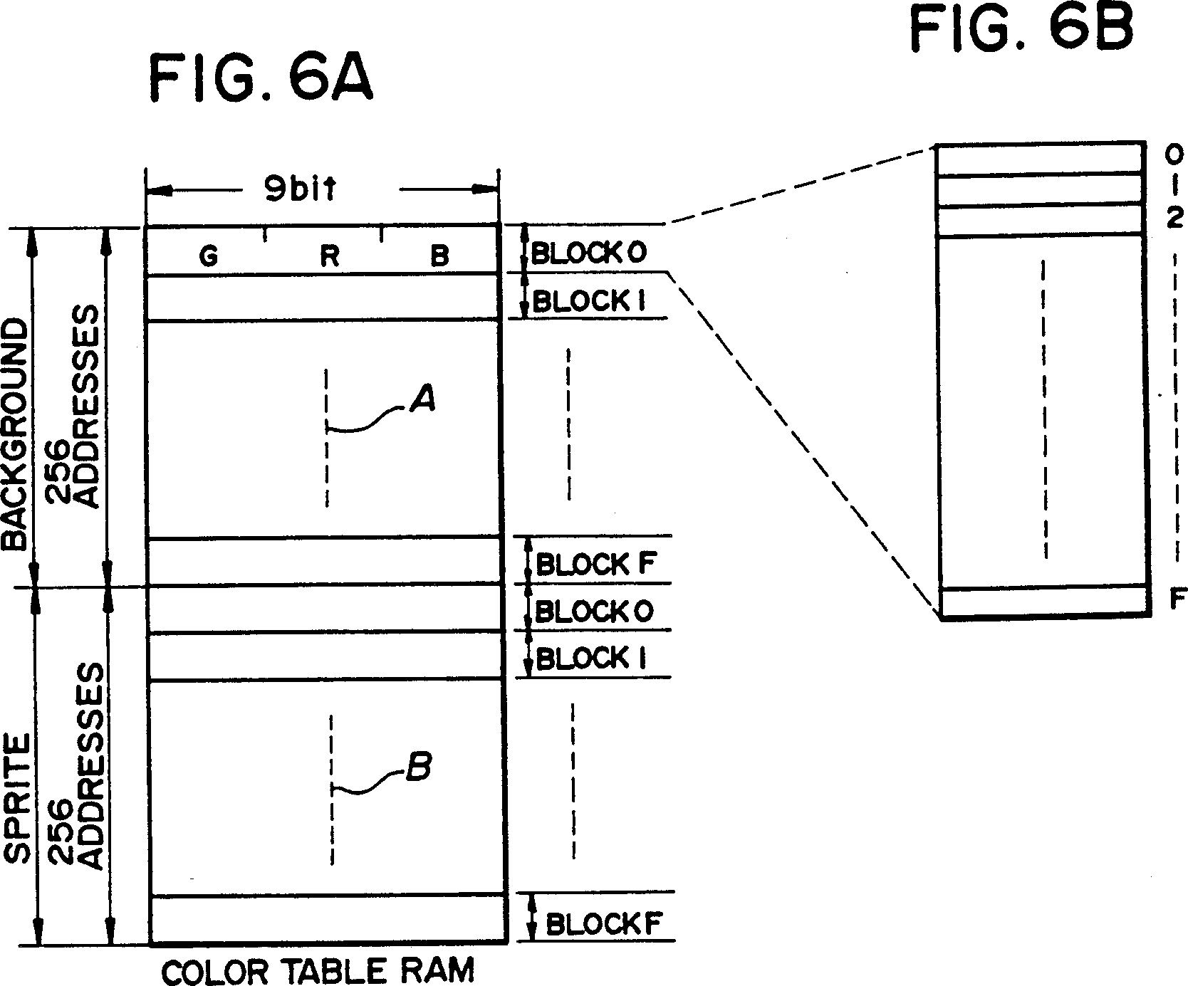
Figures 6A and 6B: Explanatory diagrams showing the color table RAM.
[Figures 6A and 6B] show the color table RAM (26) in which a region A includes color data for a background, and a region B includes color data for sprites. The regions A and B includes 16 blocks O to F each including 16 addresses 0 to F. The color table RAM (26) includes a memory region for color data R, G and B each being of 3 bits. As apparent from the above, the regions A and B have 256 addresses respectively so that 512 colors can be displayed.

Figure 7: Diagram showing a matrix ROM.
[Figure 7] shows the matrix ROM (31) which stores luminance signals Y, color difference signals B-Y and R-Y at addresses of R, G an B color signals read from the color table RAM (26) to be latched in the latch circuit (27). For instance, when the color data are that G is 000, R is 000, and B is 010, the color difference signals B-Y and R-Y are 0x14 and 0x0F, and the luminance signal is 0x01.
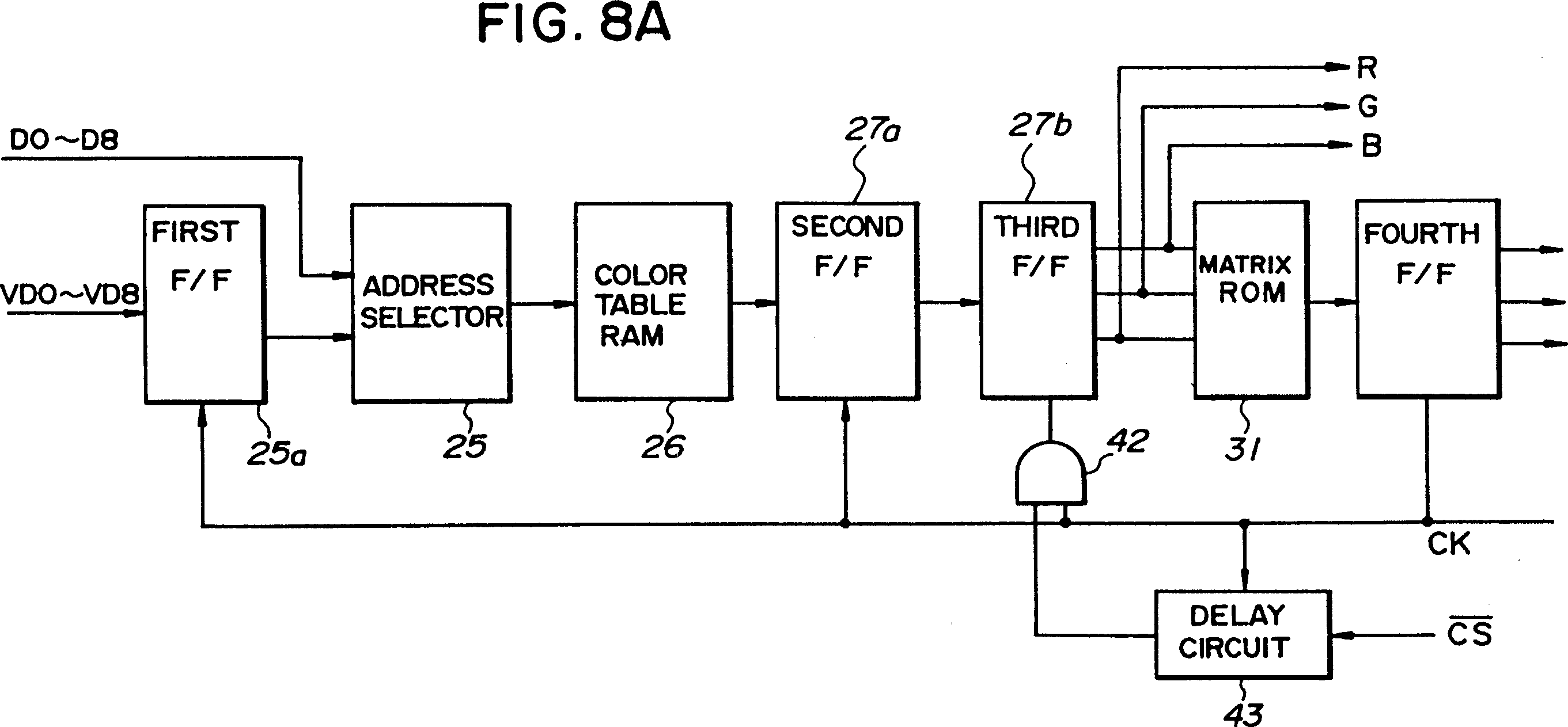

Figure 8A: Block diagram of the Video Color Encoder.
Figure 8B: Timing chart of the apparatus in operation.
[Figure 8A] shows the address selector (25), the color table RAM (26) and the matrix ROM (31) as shown in [Figure 2]. A first flip-flop (25a) is provided to function as a latch circuit at a front stage of the address selector (25), and second and third flip-flops (27a and 27b) are provided as the latch circuit (27) in [Figure 2] at a rear stage of the color table RAM (26). The operation of the first to third flip-flops (25a, 27a and 27b) are controlled with timings of pixel clocks (CK), provided tat the third flip-flop (27b) is controlled with pixel clocks (CK) passed through an AND circuit (42) having two inputs connected to a pixel clock terminal and a delay circuit (43). The delay circuit (43) produces a signal 0 when the chip selection signal (CS) is 0, and a signal 1 when a predetermined time T is elapsed after the chip selection signal (CS) becomes 1 from 0. A fourth flip-flop is connected to an output of the matrix ROM (31).
In operation, color data are first written into the color table RAM (26) through a process in which the Color Table Address register (CTA) is addressed with address signals A1 and A2 of 1 and 0 so that a starting address CTA of the color table RAM (26) is set therein. In a case where the 16 bit width is selected, the starting address is set by one time. While, in a case where the 8 bit width is selected, the starting address is set in such a manner that a lower byte is first set therein and an upper byte is then set therein. Next, color data are written into the color table RAM (26) at the address in such a manner that the color data are written thereinto by one time in case of 16 bit width, while a lower byte thereof and then an upper byte thereof are written thereinto in case of 8 bit width. Then, an address of the color table RAM (26) is automatically incremented so that color data are successively written thereinto.
When video data as shown in [Figure 5] are transferred through the VDC data bus (22) from the Video Display Controller (5) to the Video Color Encoder (4), the address selector (25) selects the transferred video data to decide an address of the color table RAM (26) as shown in [Figures 6A and 6B] so that color data of R, G and B are read therefrom to be latched in the latch circuit (27) in accordance with the pixel clock (CK). At this moment, one of regions A and B is selected dependent on a content of the VD8 bit as described before, and a predetermined block is selected in the selected region A or B dependent on a content of the VD4 to VD7 bits. In the selected block, a predetermined address is accessed dependent on a content of the VD0 to VD3 bits. When color data are latched in the latch circuit (27), analog RGB signals or a composite signal can be supplied from the analog RGB signal output circuit (41A) or the composite signal output circuit (41B) through the interface 7 or 8 to the video display (9).
-
Output of analog RGB signals When the frequency dividing ratio PCC of the Control Register (CR) is set to be 0x01, the frequency dividing ratio is three as shown in [Figure 4]. Digital RGB color data in the latch circuit (27) are converted in the R, G and B digital to analog converters (28, 29 and 30) to produce analog RGB signals. Simultaneously, horizontal and vertical synchronous signals HSYNC and VSYNC supplied from the synchronous signal producing circuit (33) are combined in the synchronous signal composite circuit (34) to produce a composite synchronous signal. Then, these analog RGB and composite synchronous signals are supplied from the analog RGB signal output circuit (41A) directly to the video display (9) or to an exclusively used monitor means (not shown). The analog RGB signals thus supplied thereto are of a video band of 7 MHz. On the contrary, the video band will be 5 MHz, if the frequency dividing ratio is set to four.
-
Output of a composite signal
When the dividing ratio PCC of the Control Register (CR) is set to be 0x00, the dividing ratio is four. A luminance signal Y and color difference signals R-Y and B-Y are supplied from the matrix ROM in accordance with R, G and B color data latched in the latch circuit (27), and then converted in the digital to analog converters 35, 36 and 37 to analog signals. At this moment, the luminance signals Y are combined with the synchronous signals from the synchronous signal producing circuit (33). On the other hand, color carriers are obtained from the balanced modulation of color subcarriers having the same frequency and different phases by ninety degrees, which are supplied from the synchronous signal producing circuit (33) in accordance with the color difference signals R-Y and B-Y. Further, a burst signal is obtained from the insertion of the color subcarrier of 8 or nine cycles into a back porch period of the horizontal synchronous signal in the burst signal producing circuit 40. These signals thus obtained are combined in the composite signal output circuit (41B) to produce a composite signal which is then supplied through the interface (8) to a receiving circuit of the video display (9) to be displayed on the video display thereof. The composite signal is of a video band of 5 MHz and is based on a system of NTSC. As a matter of course, the video band may be 7 MHz as described before.
Next, a timing at which RGB color data are latched in the latch circuit (27) with the pixel clock (CK) will be described in more detail in conjunction with [Figures 8A and 8B].
When video data VD0 to VD8 are transferred from the Video Display Controller (5) to the Video Color Encoder (4), the video data are latched in the first flip-flop (25a), and the color table RAM (26) is addressed with an address signal of the video data VD0 to VD8 so that RGB color data are read from the color table RAM (26) to be latched in the second flip-flop (27a). When a first bit of the second flip-flop (27a) is latched in the third flip-flop (27b), it is assumed that the chip selection signal (CS) becomes 0 for the purpose that data are written into the color table RAM (26) by the CPU (1). As a result, an output of the delay circuit (43) becomes 0 to result in no output of the pixel clock (CK) from the AND circuit (42). Therefore, a second bit and signals following after the second bit in the second flip-flop (27a) are prevented from being latched in the third flip-flop (27b). Thereafter, when the chip selection signal (CS) becomes " 1", the delay circuit (43) times a predetermined time T, and when the time T is elapsed, an output of the delay circuit (43) becomes 1. Accordingly, the pixel clock (CK) is again supplied to the third flip-flop (27b) so that an 8 bit and signals following after the 8 bit in the second flip-flop (27a) are latched in the third flip-flop (27b) to be supplied to a following stage as digital RGB signals. At this moment, an output of RGB color data is prohibited during an indeterminate period of data in the color table RAM (26) so that flicker caused by a transfer of data between the CPU (1) and the color table RAM (26) is prevented from being occurred on the display. In the color table RAM (26), one of the regions A and B is selected dependent on a content of the VD8 bit, and one of blocks is selected dependent on a content of the VD4 to VD7 bits in the selected region A or B. In the selected block, one of addresses is accessed dependent on a content of the VD0 to VD3 bit. When color data are latched in the third flip-flop (27b), analog RGB signals and a composite signal can be produced as described before.
Although the invention has been described with respect to specific embodiments for complete and clear disclosure, the appended claims are not thus limited but are to be construed as embodying all modifications and alternative constructions that may occur to one skilled in the art which fairly fall within the basic teaching herein set forth.
What is claimed is:
-
An apparatus for providing video signals, comprising:
- A color table RAM for storing RGB color data at addresses defined by video data, said addresses including:
- A first group of addresses for background RGB color data.
- A second group of addresses for sprite RGB color data.
- Each group of addresses includes plural blocks, each containing plural addresses.
The video data includes:- A bit designating one of the first and second groups.
- A predetermined number of bits designating one of the plural blocks.
- A predetermined number of bits designating an address in a designated block.
- A circuit for supplying RGB analog signals to a display means selected from:
- A video display of a television set.
- An RGB monitor.
- Said RGB analog signals are obtained by a digital-to-analog conversion of RGB color data read from the color table RAM.
- A matrix ROM for storing luminance signals and color difference signals at addresses each defined by said RGB color data.
- Addresses of the matrix ROM are designated by RGB color data read from the color table RAM.
- A circuit for supplying a composite signal to a receiving circuit of a television set.
- Said composite signal is obtained by:
- An analog luminance signal to which a luminance signal read from the matrix ROM is converted.
- Color carriers generated from analog color difference signals, to which color difference signals read from the matrix ROM are converted, in accordance with a modulation by use of color subcarriers.
- Said composite signal is obtained by:
- A color table RAM for storing RGB color data at addresses defined by video data, said addresses including:
-
An apparatus for producing video signals according to claim 1 further comprising means for:
- Transferring said RGB color data to said color table RAM for storing said data.
- Producing a delay signal for a predetermined time after a transfer of said RGB color data is finished by said means for transferring.
- Inhibiting a display of said RGB color data read from said color table RAM during:
- A transfer period of said RGB color data.
- An output period of said delay signal.
-
An apparatus for producing video signals according to claim 2, wherein said means for inhibiting includes:
- A latch circuit for latching said RGB color data in accordance with a pixel clock.
- A gate circuit for inhibiting supply of an output from said pixel clock to said latch circuit during said output period.