Arcade Card
The Arcade Card is an expansion HuCard for the PC Engine intended to be used with the CD-ROM² hardware. The card comes in two varieties:
- Arcade Card Pro: Includes 256KB extra RAM and the Super CD-ROM² System 3.1 BIOS for non-Duo PC-Engines.
- Arcade Card Duo: Does not include extra RAM and is used with a Duo console.
It is unknown if the Duo version of the Arcade Card contains the CD-ROM² BIOS. Both types include:
- 2 MB of non-memory-mapped RAM.
- A collection of registers to access the 2 MB RAM in various patterns.
- A 32-bit-wide programmable shift register.
The Arcade Card has four individual port registers to access the 2 MB of memory. Each register operates independently and can overlap without conflict.
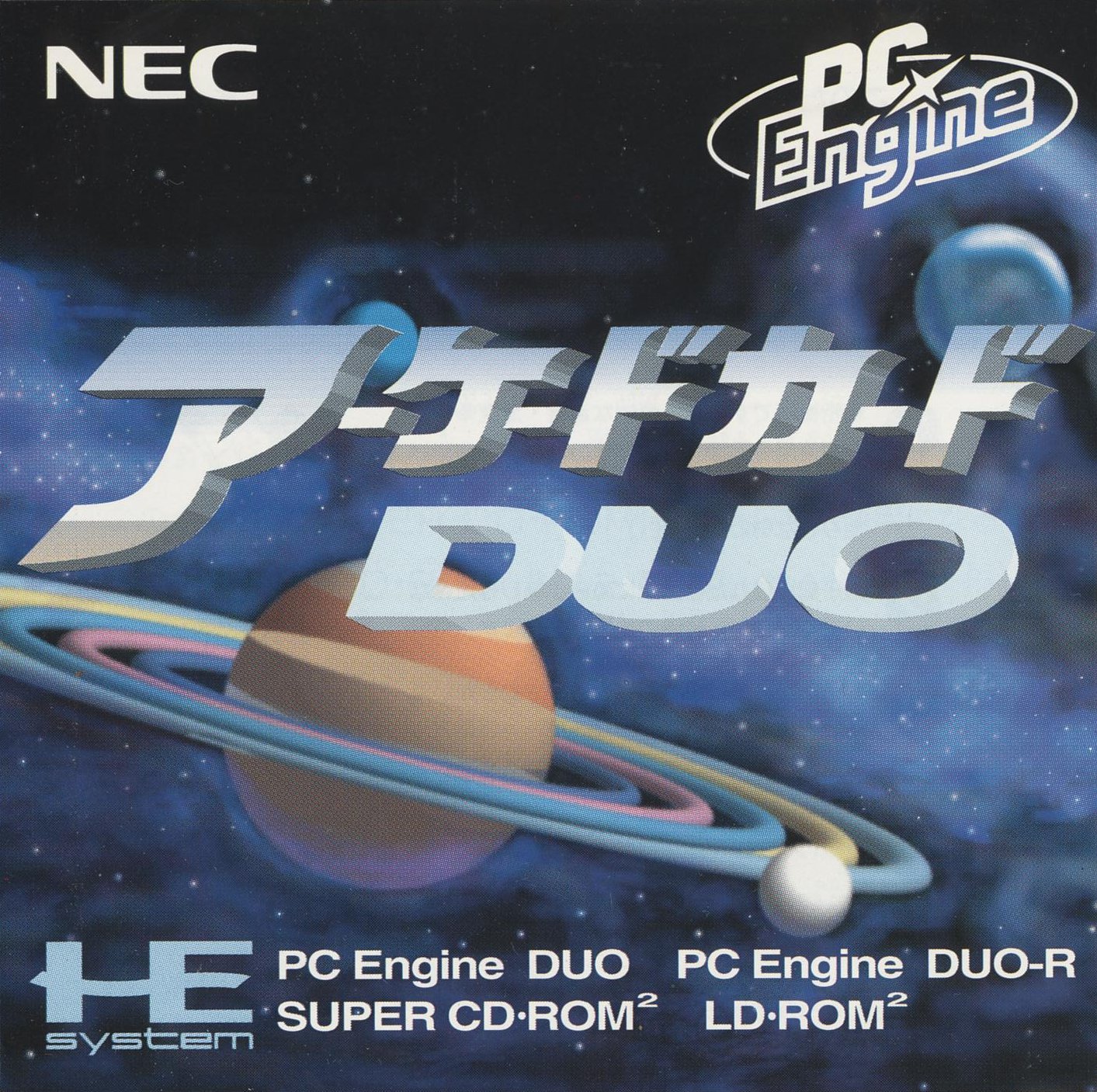
Cover of Arcade Card Duo case

Arcade Card Duo for Turbo Duo

Cover of Arcade Card Pro case

Arcade Card Pro for Super CD·ROM²
The Arcade Card has four sets of memory-mapped registers:
| Address | Name |
|---|---|
$1A00 |
Port 1 |
$1A10 |
Port 2 |
$1A20 |
Port 3 |
$1A30 |
Port 4 |
Each port register consists of the following:
| Byte | Description |
|---|---|
| 0/1 | Data read/write registers. |
| 2/3/4 | Base address of the 2 MB range. Format is 24-bit: low, middle, high byte. |
| 5/6 | Offset register. Format is 16-bit LSB/MSB. |
| 7/8 | Increment register. Format is 16-bit LSB/MSB. |
| 9 | Control register. |
| 10 | Manual Offset Trigger. Any write to this register triggers adding the offset to the base address. |
The Data port register acts as an address register. It uses the value of the Base register for address calculation to point into Arcade Card memory. All access to the Arcade Card memory goes through these register sets. Depending on the bits set in the control register, different address calculation configurations can be used.
- The Offset register can index the Base register.
- Either the Base or Offset register can be configured to auto-increment or decrement upon access to these Data registers.
The Offset register functions as a "window" or "index" register. It can be configured to add its value to the Base register during address calculation for memory fetch/store operations.
-
Key Behaviors:
- The Offset register does not accumulate back into the Base register on every Data register access.
- When D1 of the Control register is set, the Offset behaves as described above.
- Byte 10 allows manual addition of the Offset register's value to the Base register. This happens on each write to byte 10, regardless of the value written.
-
Note: When D6/D5 of the Control register are set to values other than
%00, this addition is applied during Data port access.
-
Note: When D6/D5 of the Control register are set to values other than
-
The Offset register can increment or add only to specific bytes in the Data register set. This is useful for incrementing on WORD-sized read/write operations.
-
Control register bit D3 determines how the 16-bit Offset register value is interpreted:
- If D3 is set, the Offset register is treated as a signed number for indexing and addition functions.
Control register bits D2 and D3 determine how Offset and Increment register values are treated.
- When set to signed, values are interpreted as 2's complement.
- Signed status affects the addition of Offset or Increment values to the Base register:
- Base is 24-bit, while Offset and Increment registers are 16-bit.
- Offset and Increment values are sign-extended to 24 bits before being applied to the Base register.
When Control register bit D0 is set, auto-increment occurs on every read/write of the Data register set.
-
Increment Register:
- Holds the value to be added to another register.
- Control bit D4 specifies whether the Base or Offset register is incremented.
- Control register bit D2 determines whether the Increment value is sign-extended to 24 bits before being added to the Base register.
When Control register bit D4 is set to "Offset," the Increment register is added to the Offset register. The Base register remains unaffected.
Example Use Case: Fatal Fury Special uses this Arcade Card register block as a 16-bit down counter.
assembly
; Byte7/8 = $FFFF (-1)
; Byte9 = %101 (offset auto-increment on, Byte7/8 treated as signed)
loop:
  lda $1a10     ; Triggers the auto-increment
  lda $1a15
  ora $1a16     ; If both LSB and MSB of Offset are $0000, then loop finished.
  bne loop
rts
These registers have specific memory locations and are not grouped like the previously mentioned set of registers.
| Address | Length | Description |
|---|---|---|
$1AE0 |
4 bytes | A 32-bit register. Format: lowest, low, mid, high byte. |
$1AE4 |
1 byte | Amount to shift the 32-bit register. Lower four bits are signed. |
$1AE5 |
1 byte | Amount to rotate the 32-bit register. Lower four bits are signed. |
$1AEC |
2 bytes | Should return $00/00. |
$1AFE |
1 byte | When read, gives the version number of the Arcade Card. |
$1AFF |
1 byte | Arcade Card ID = $51. Used to detect the card. |
- The last byte (
$1AE3) is a latch. Writing to this byte copies all four bytes into an internal 32-bit register. - Reading back from this byte also activates the latch mechanism. For example:
- You can write to one of the lower 3 bytes and then read from the last byte to update the register.
- The value in the 32-bit register is always treated as unsigned when the shift logic is applied.
- The register is 8 bits, but only the lower 4 bits are used for shift/rotate operations.
- The upper 4 bits are retained in the register and can be read back.
- The lower 4 bits are signed, controlling the direction of the shift/rotate.
- Writing to these two registers activates the shift mechanism/logic.
Four banks of Data registers mirrored throughout an 8K memory space. Each bank corresponds to one of the four Address register sets.
| Bank | Description |
|---|---|
$40 |
Data registers 0/1 of $1A00 mirrored in the 8K bank. |
$41 |
Data registers 0/1 of $1A10 mirrored in the 8K bank. |
$42 |
Data registers 0/1 of $1A20 mirrored in the 8K bank. |
$43 |
Data registers 0/1 of $1A30 mirrored in the 8K bank. |
The mirrored registers serve a specific purpose. They allow the use of the Txx block transfer instructions with the Data register ports. However, there are no port-to-port block transfer instructions. To achieve Arcade Card port reads to VDC port writes, a special Txx instruction (which doesn't exist) would normally be required. A clever workaround is to organize a set of ports so that they can be read in sequential order, simulating normal sequential linear addressing.
These ports are mirrored sequentially within a single 8KB block. This works for both HuC6270 to Arcade Card and Arcade Card to HuC6270 transfers. The greater benefit is for transferring data to VRAM. Each bank of $40-43 corresponds to one of the four sets of Arcade Card Data registers.
Key Points:
- You are limited to 8KB per Txx single transfer. For transfers larger than 8KB, remap the same bank number to the next page register(s).
- To transfer data to VRAM, use the normal TIA (Transfer Increment Alternate) instruction.
- To read from VRAM to Arcade Card, use the TAI (Transfer Alternate Increment) instruction.
Each port register is defined as follows:
| Byte | Description |
|---|---|
| Byte 0 | 1-byte-wide read/write port access into the Arcade Card memory. Byte 0 and 1 are the same port (useful for TIA and TAI instructions). |
| Byte 2-4 | The 24-bit address of the Arcade Card memory. The order is: low byte, medium byte, high byte. |
| Byte 5-6 | Offset for use with base offset address mode. The order is LSB/MSB. |
| Byte 7-8 | Incrementor value (LSB/MSB). If the increment flag is enabled, the address register will be incremented by this value. |
| Byte 9 | Control register: |
| - Bit 7: N/A | |
| - Bit 6: Allow writes to Byte 6 to add offset to base (only if Bit 5 is clear). | |
| - Bit 5: Allow writes to Byte 10 to add offset to base (only if Bit 6 is set). |
set-bit 4 auto-increment flag:
  0 - Increment offset
  1 - Increment base

Bit 3: Auto-decrement.
Bit 2: Signed extension for offset.

The shift register is located at $1AE4, with data (4 bytes in length) located at $1AE0.
-
$1AE4: The number of bits to shift. Negative values shift right, and positive values shift left. -
$1AE5: Simple 8-bit latch.
Four banks of Data registers mirrored throughout an 8KB memory block. Each bank corresponds to one of the four Address register sets.
| Bank | Description |
|---|---|
$40 |
Data registers 0/1 of $1A00 mirrored in the 8KB bank. |
$41 |
Data registers 0/1 of $1A10 mirrored in the 8KB bank. |
$42 |
Data registers 0/1 of $1A20 mirrored in the 8KB bank. |
$43 |
Data registers 0/1 of $1A30 mirrored in the 8KB bank. |
With this method, the TIA instruction can transfer data from the Arcade Card memory to HuC6270 VRAM directly. The TAI instruction can transfer data from VRAM to Arcade Card memory. You can also use this method to read directly from the CD into the Arcade Card memory using the CD_READ function with the MPR argument and any Arcade Card bank:
-
$40: Arcade Card port register 1 -
$41: Arcade Card port register 2 -
$42: Arcade Card port register 3 -
$43: Arcade Card port register 4