Patent 4951038
Note: This patent has been augmented with information and drawings from Patent 5319786.
Note: All mentions of "dot" have been replaced with "pixel" (DCC is now PCC).
Note: Terminals with a High value are a binary 1 and Low is a binary 0.
United States Patent Number: 4951038
APPARATUS FOR DISPLAYING A SPRITE ON A SCREEN
Apparatus for displaying a sprite on a screen comprises Sprite Attribute Tables each including coordinates indicating a display position of a sprite, a pattern code defining the sprite in regard to pattern data, and control data defining a display mode of the sprite. A Sprite Generator is addressed in accordance with the pattern code to supply the pattern data of a sprite to a pattern data buffer. The sprite is displayed in accordance with the coordinates thereof on the screen. Therefore, the sprite is moved on the screen only by changing the coordinates of a corresponding Sprite Attribute Table.
The invention relates to an apparatus for displaying a sprite on a screen, and more particularly to an apparatus for displaying a sprite on a screen in which an image unit composed of a plurality of pixels, which is called a sprite, is moved to be displayed on such a screen as a video display and so on.
One of the apparatuses for displaying an image unit composed of a plurality of pixels on a video display is described in Japanese Patent Laid-open No. 11390/1982. In the apparatus for displaying an image unit on a video display, the image unit is moved on the video display in accordance with the subtraction between the X value of standard coordinates of the image unit and a vertical standard line, and between the Y value of the standard coordinates and a horizontal standard line. In controlling the image unit to be moved on the video display, control signals for two adjacent horizontal scanning lines are alternately written into two line buffer memories which are provided in parallel and alternately read from the memories so that image signals read from a character image memory are processed in accordance with the control signals thus read from the line buffer memories, thereby being displayed on the video display. The control signals comprise signals of the aforementioned subtractions in the X and Y directions so that the image unit is moved smoothly on the video display by increasing or decreasing the subtraction signal at an appropriate displaying time.
According to the apparatus for displaying an image unit on a video display, however, there is a disadvantage that a memory region is increased because the character image memory is accessed after the control signals for the image unit are once written into the parallel line buffer memories.
There is a further disadvantage that enlarging the size of an image unit is difficult to perform.
There is a still further disadvantage that, where the number of image units designated to be displayed on a video display exceeds a predetermined number, an image unit exceeding the predetermined number is not displayed on the video display.
There is yet another disadvantage that there are provided additional registers into which the so-called "blanking mode" instruction is stored to perform the blanking mode, wherein an image unit is moved from the edge of a video display to appear thereon or is moved to the edge thereof to disappear therefrom.
Accordingly, it is an object of the invention to provide an apparatus for displaying a sprite on a screen in which line buffer memories for storing control signals for a sprite are not necessary to be provided.
It is a further object of the invention to provide an apparatus for displaying a sprite on a screen in which the size of a sprite is easily controlled to be changed on a screen.
It is a still further object of the invention to provide an apparatus for displaying a sprite on a screen in which, where sprites more than a predetermined number to be displayed on a single horizontal scanning line are designated, the occurrence of such a designation is indicated.
It is a yet still further object of the invention to provide an apparatus for displaying a sprite on a screen in which the aforementioned blanking mode is easily performed.
According to the invention, an apparatus for displaying a sprite on a screen comprises:
-
Sprite Attribute Tables each including:
- Coordinates indicating a display position of a sprite.
- A pattern code defining the sprite in regard to pattern data.
- Control data defining a display mode of the sprite.
- First detection means for comparing a vertical position value of the coordinates with a raster number to detect a sprite to be displayed.
- A Sprite Generator storing pattern data of the sprite.
- Second detection means for comparing a horizontal position value of the coordinates of the sprite to be displayed with a pixel clock signal to detect pattern data to be displayed.
- Means for controlling the screen to display the sprite to be displayed thereon in accordance with the pattern data to be displayed.
In Figure 1, there is shown an apparatus for displaying an image on a screen which is mainly composed of a Video Display Controller (1), a CPU (2), a Video Color Encoder (3), and a Programmable Sound Generator (4). The Video Display Controller (1) supplies the Video Color Encoder (3) with image data for a story which are read from a VRAM (7) under the control of the CPU (2) reading a program stored in a ROM (5). The CPU (2) controls a RAM (6) to store data, calculation or arithmetical results, etc., temporarily in accordance with a program stored in the ROM (5).
The Video Color Encoder (3) is supplied with image data to produce RGB analog signals or video color signals including luminance signals and color difference signals to which the RGB signals are matrix-converted by using color data stored therein. The Programmable Sound Generator (4) is controlled by the CPU (2) reading a program stored in the ROM (5) to produce audio signals making left and right stereo sounds. The video color signals produced at the Video Color Encoder (3) are composite signals supplied through an interface (8) to a video display (9), while the RGB analog signals are directly supplied to video display (9), which is used as an exclusive monitor apparatus. The left and right analog signals supplied from the Programmable Sound Generator (4) are amplified at amplifiers 11a and 11b to make sounds at speakers 12a and 12b.

Figure 1: A block diagram showing an apparatus for displaying an image on a screen in which an apparatus for displaying a sprite on a screen according to the invention is included.
In Figure 2A, there is shown the Video Display Controller (1) transferring data between the CPU (2) and VRAM (7), which comprises:
- A control unit (20) including various kinds of registers to be described later.
- An address unit (21).
- A CPU read/write buffer (22).
- A sprite shift register (24).
- A background shift register (25).
- A data bus buffer (26).
- A synchronic circuit (27).
- A priority circuit (28).
The control unit (20) is provided with:
- A [BUSY] terminal being Low to keep the CPU (2) writing data into the VRAM (7) or reading data therefrom in a case where the Video Display Controller (1) is not in time for the writing or reading of the data.
- An [IRQ] terminal supplying an interruption request signal.
- A CK terminal receiving a clock signal of a frequency for one pixel (one picture element).
- A [RESET] terminal receiving a reset signal for initializing the Video Display Controller (1).
- An EX 8/[16] terminal receiving a data bus width signal for selecting one of 8- and 16-bit data buses.
The address unit (21) is connected to terminals MA0 to MA15 supplying address signals for the VRAM (7), which has, for instance, a special address region of 65,536 words. The address unit (21), CPU read/write buffer (22), Sprite Attribute Table (23), sprite shift register (24), and background shift register (25) are connected to terminals MD0 to MD15 through which data are transferred to and from the VRAM (7).
- The Sprite Attribute Table buffer (23) is a memory for storing X and Y display positions, pattern codes, and control data of sprites, each composed of 16×16 pixels.
- The sprite shift register (24) stores pattern and color data of a sprite read from a Sprite Generator in the VRAM (7), which is accessed in accordance with the pattern codes stored in the Sprite Attribute Table (23).
- The background shift register (25) stores pattern data, along with CG color, read from a character generator in the VRAM (7) in accordance with an address based on a character code of a Background Attribute Table in the VRAM (7).
The data bus buffer (26) is connected to terminals D0 to D15 through which data are supplied and received. In the Video Display Controller (1), an 8- or 16-bit interface is selected to comply with a data width of a system including the CPU (2), wherein the terminals D0 to D7 among the terminals D0 to D15 are occupied when the 8-bit interface is selected.
The synchronic circuit (27) is connected to:
- A DISP terminal indicating a display period.
- A [VSYNC] terminal supplying a vertical synchronous signal for a video display (9) and receiving an external vertical synchronous signal.
- A [HSYNC] terminal supplying a horizontal synchronous signal for a video display (9) and receiving an external horizontal synchronous signal.
The priority circuit (28) is connected to terminals VD0 to VD7 through which video signals are supplied, and a SP/BG (VD8) terminal being High when the video signals are of a sprite and Low when the video signals are of a background.

Figure 2A: A block diagram showing a Video Display Controller for the control of writing video signals into VRAM and reading video signals therefrom.
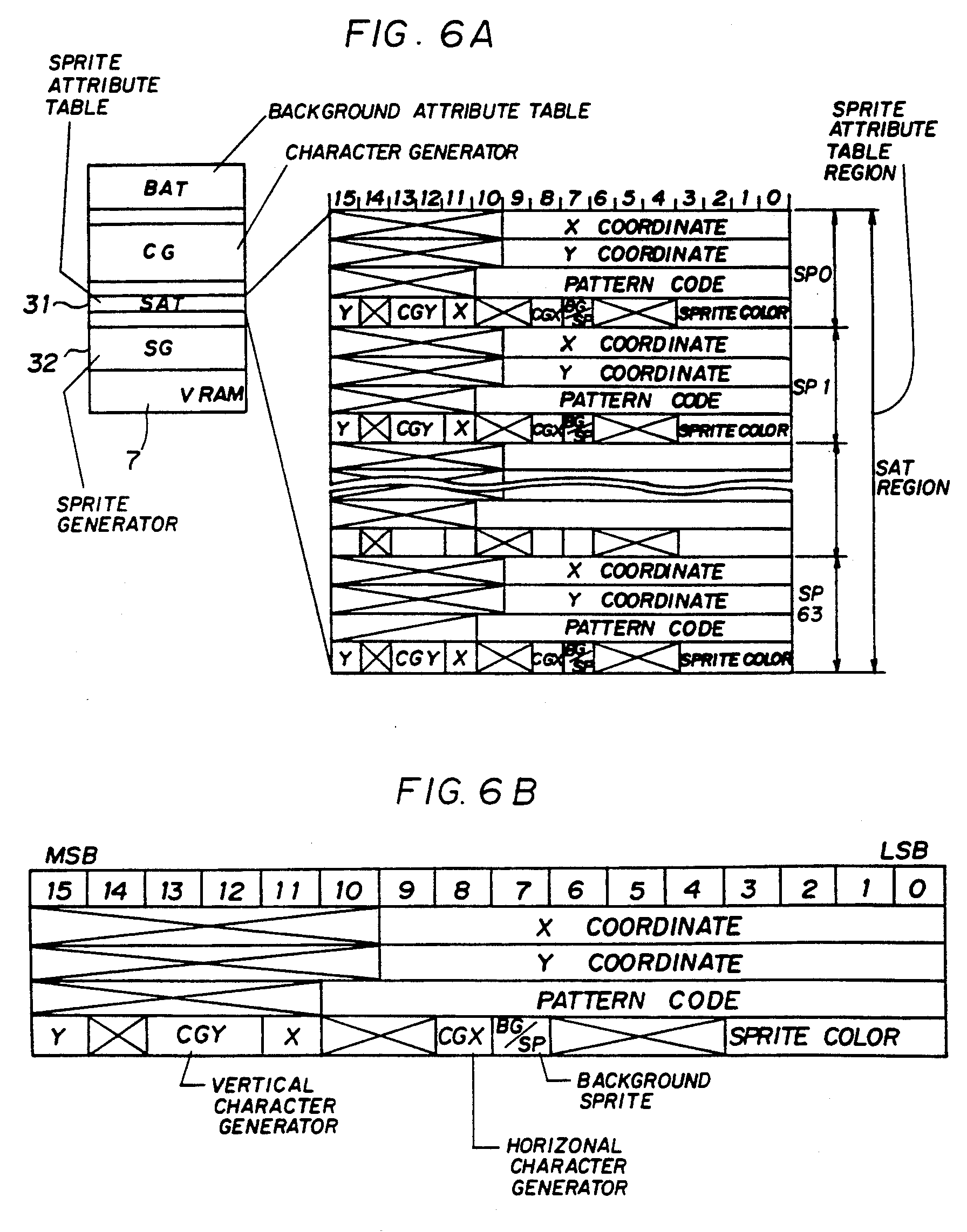
In Figure 2B, there is shown an apparatus for displaying a sprite on a screen in an embodiment according to the invention wherein the reference numerals 31 and 32 indicate a Sprite Attribute Table and Sprite Generator in the VRAM (7), respectively. The Sprite Attribute Table (31) can include, for instance, 64 sprites, while the Sprite Generator (32) can include, for instance, 1,024 sprites.
- In the Sprite Attribute Table (31), addresses of 0 to 63 are assigned to the 64 sprites to give a priority in the order of 0 > 1 > ... > 62 > 63.
- Each sprite is composed of 16×16 bits and includes X and Y coordinates, pattern codes, and control data.
As to each of the sprites:
-
The Y coordinate is compared with a raster signal supplied from a scanning raster producing circuit 33 in a coincidence detection circuit (34). Sprites with a Y coordinate coincident with a raster signal are stored in a pattern code buffer (35), which can store up to 16 sprites, by referring to a corresponding address (0 to 63).
-
A selector (36) selects a pattern code from the Sprite Attribute Table (31) in accordance with an address stored in the pattern code buffer (35).
-
The selected pattern code accesses the Sprite Generator (32) at a corresponding address, thereby reading pattern data.
-
The pattern data thus obtained are stored into a pattern data buffer (37) along with an X coordinate corresponding thereto read from the Sprite Attribute Table (31).
-
Storing of sprites into the pattern code buffer (35) is performed at a horizontal display period preceding the present horizontal display period by one scanning raster.
-
Storing of pattern data into the pattern data buffer (37) is performed at the following horizontal retrace period.
When a scanning raster for displaying pattern data occurs:
- The X coordinate stored in the pattern data buffer (37) is compared with a counted value of a horizontal pixel clock counter (PCC) (38) in a coincidence detection circuit (39).
- Pattern data with an X coordinate coincident with the counted value are supplied to a parallel/serial converting circuit (40).
- In the parallel/serial converting circuit (40), parallel pattern data are converted into serial pattern data, which are supplied through a gate circuit (42) to a video display (9).
- The gate circuit (42) is controlled to turn on/off in accordance with the content of a starting coordinates registration circuit (43) defined by the CPU (2).

Figure 2B: A block diagram showing an apparatus for displaying a sprite on a screen in an embodiment according to the invention.
In Figure 4A, there is shown an address in a Background Attribute Table for a character on a fictitious screen. A character and color to be displayed at each character position are stored in the Background Attribute Table. A predetermined number of Background Attribute Tables are stored in a region, the first address of which is 0 in the VRAM (7). The fictitious screen shown therein, which is one example, is of 32×32 characters.

Figure 4A: An explanatory diagram showing a fictitious screen in the embodiment according to the invention.
In Figure 4B, there is shown a screen framed by writing respective predetermined values into the Horizontal Synchronous Register, Horizontal Display Register, vertical synchronous register, and Vertical Display Register as shown in Figures 3L, 3M, 3N, and 30. Although the respective predetermined values for the registers are not explained here, a display region is defined in accordance with HDW + 1 in the Horizontal Display Register and VDW + 1 in the Vertical Display Register. In the embodiment, the starting coordinates (x, y) for the display region are indicated as (32, 64).

Figure 4B: An explanatory diagram showing a display region on a screen in the embodiment according to the invention.
In Figures 5A and 5B, there are shown Background Attribute Tables (BATs) in the VRAM (7), each of 16 bits, containing:
- A character code (lower 12 bits) for designating a pattern number of a character.
- A CG color (upper 4 bits) for designating a CG color code.

Figures 5A and 5B: Explanatory diagrams showing a Background Attribute Table in the VRAM in the embodiment according to the invention.
In Figures 6A and 6B, there are shown Sprite Attribute Tables (SATs) (31) in the VRAM along with a Sprite Generator (32). Each Sprite Attribute Table (31) is composed of 16 × 4 bits, or four words, to define a sprite. Therefore, 64 sprites are defined by 256 words.
- In the Sprite Attribute Table:
- Lower 10 bits in the first word designate a horizontal position (0 to 1023) of a sprite.
- Lower 10 bits in the second word designate a vertical position (0 to 1023) of a sprite.
- Lower 11 bits in the third word designate a pattern number, which is an address for the Sprite Generator (32).
- The fourth word is for control bits, including:
- [Y] (X₁₅): Sprite is reversed in the Y direction.
- CGY (2 bits: X₁₃ and X₁₂): Defines three modes (described later).
- (X₁₁): Sprite is reversed in the X direction.
- CGX (X₈): Joins two sprites horizontally.
-
SP/BG (X₇): Priority between background and sprite:
- 0 - Background.
- 1 - Sprite.
- Sprite color (X₃ to X₀): Area color of a sprite.
Each sprite has four facets, called SG0 to SG3, each being 16×16 pixels, occupying 64 words.

Figures 6A and 6B: Explanatory diagrams showing a Sprite Attribute Table in the embodiment.
The writing of data into a Sprite Attribute Table (31) is performed through DMA transfer from the CPU (2) to the Sprite Attribute Table buffer (23) instead of directly transferring the data from the CPU (2) to the VRAM (7).
In operation, a sprite SP having standard coordinates (2, 2) is displayed on a video display (9) with 1024 display pixels in both X and Y directions, as shown in Figure 7. In displaying the sprite SP, the Y coordinates of the 64 Sprite Attribute Tables (31) are compared in turn with a raster signal supplied from the scanning raster signal producing circuit (33) at the coincidence detection circuit (34). Sprites with a Y coordinate of 2 are stored in their stripe number (0 to 63) into the pattern code buffer (35) when the horizontal display period of a scanning raster number 1 begins, as shown in Figure 2B.
A maximum of 16 sprites can be stored in the pattern code buffer (35). During a horizontal retrace period (after scanning raster number 1 ends and before scanning raster number 2 begins), address signals are produced in the selector (36) based on sprite numbers stored in the pattern code buffer (35) and pattern codes in the Sprite Attribute Tables (31). These address signals are used to read pattern data from the Sprite Generator (32), which are then stored in the pattern data buffer (37) along with the corresponding X coordinates from the Sprite Attribute Tables (31).
When the horizontal display period of scanning raster number 2 starts, the X coordinates stored in the pattern data buffer (37) are compared with counted values from the horizontal pixel clock counter (38) in the coincidence detection circuit (39). Pattern data for the sprite SP are read and supplied to the parallel/serial converting circuit (40) when the counted value corresponds to x=2. Parallel pattern data are converted into serial pattern data in the parallel/serial converting circuit (40), allowing the sprite SP's picture element (2, 2) to be displayed on the video display (9) through the gate circuit (42). Subsequently, the picture elements (3, 2), (4, 2) ... (17, 2) are displayed, completing the display of the sprite SP on the y=2 raster line. Control data from the Sprite Attribute Table (31) corresponding to the sprite SP manage its display.
To move the sprite SP (coordinates: 2, 2) to a new display position (coordinates: x, y), becoming sprite SP', only the X and Y coordinates in the Sprite Attribute Table (31) need to be updated. The contents of the Sprite Generator (32) remain unchanged, and no redefinition of the pattern is necessary. Both sprites SP and SP' are displayed by combining one or more facets (SG0 to SG3).
The combination of facets SG0 to SG3 is illustrated in Figure 8. For instance:
- All four facets (SG0 to SG3) combine to display sprite SP₁.
- SG0 and SG1 combine to display sprite SP₂.
This results in 24 display patterns, calculated as 4 × 3 × 2 = 24. A desired pattern can be selected from these using control data in the Sprite Attribute Table. Each facet (SG0 to SG3) has a different color designated by an area color code.
Next, the CGX and CGY control data in a Sprite Attribute Table (31) are explained.
Figures 6A and 6B: Explanatory diagrams showing a Sprite Attribute Table in the VRAM in the embodiment according to the invention.

Figure 7: An explanatory diagram explaining a first operation in which a sprite is moved on a screen in the embodiment according to the invention.
In Figure 9, there is shown a Sprite Generator (SG) (32) containing pattern data A, B, C, etc. Based on the definitions of CGX and CGY (explained earlier), various sprite patterns with different colors and sizes can be generated without increasing the memory area of the Sprite Generator (32), as shown in Figures 10A to 10E.
Further explanations of [X], [Y], CGX, and CGY are provided in conjunction with Figures 11A to 11C and 12A to 12C.

Figure 8: An explanatory diagram explaining a second operation in which multiple facets are combined to form a sprite in the embodiment according to the invention.
Figure 9: An explanatory diagram showing a Sprite Generator in the embodiment according to the invention.
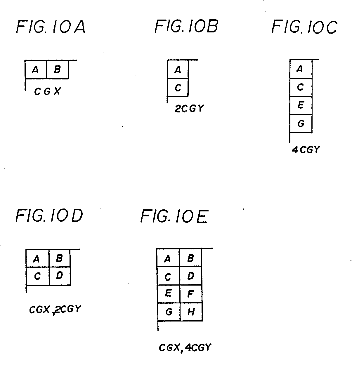
Figures 10A to 10E: Explanatory diagrams showing a third operation in which the size of a sprite is enlarged in the embodiment according to the invention.
In Figure 11A, when a bit X in a Sprite Attribute Table (31) is set to 1, a sprite is displayed reversed in a left-side-right manner. Similarly, when a bit Y in the Sprite Attribute Table (31) is set to 1, the sprite is displayed reversed upside down. If both bits X and Y are set to 1, the sprite is reversed in both directions.

Figures 11A to 12C: Explanatory diagrams showing a fourth operation in which a sprite is reversed, and multiple sprites are combined to enlarge their size in the embodiment according to the invention.
In Figures 11B and 11C, the CGX control mode is explained further. When the CGX bit is set to 1, a sprite at an address designated by a pattern code in a Sprite Attribute Table is joined with a sprite at a preceding or following address along the X direction.
For example:
- If the designated address is 00001000110 (Figure 11B), a sprite at address 00001000100 (with bit X' changed from 1 to 0) is positioned to the left.
- A sprite at the designated address (where bit X₁ is 1) is positioned to the right.
The CGX mode results in a combined sprite as shown in Figure 11C, where two patterns (X = 0, Y = 0 and X = 1, Y = 0) are displayed.
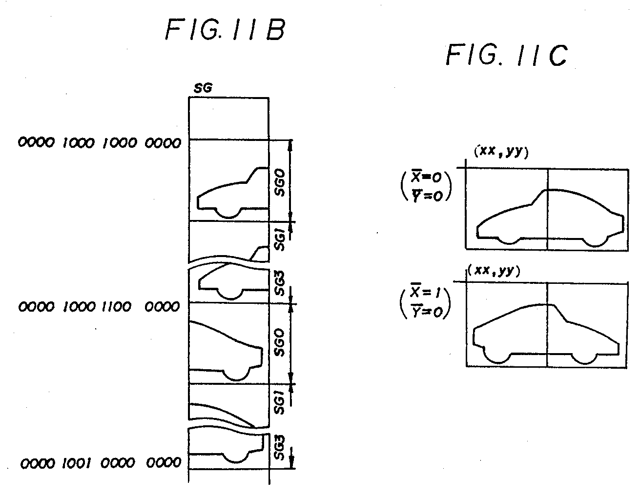
Figures 11B and 11C: Explanatory diagrams showing how sprites are combined using the CGX control mode.
In Figures 12A to 12C, the CGY display mode is explained further. In the CGY mode, the 2 bits X₃ and X₂ in a pattern code in a Sprite Attribute Table control the display, cycling through states: (0, 0), (0, 1), (1, 0), and (1, 1).
For instance:
- If the pattern code in a Sprite Attribute Table is 00001000110, the address map of a Sprite Generator is shown in Figure 12A.
- The sprite is displayed in a 4CGY mode:
- In Figure 12B, X and Y bits are not set to 1.
- In Figure 12C, the X bit is not set to 1, but the Y bit is set to 1.
In the CGX display mode, the sprite pattern size is 2 × 16 × 16 pixels, while in the 4CGY mode, it is 4 × 16 × 16 pixels. The starting coordinates (x, y) of the display region are set to (32, 64) in this embodiment. These starting coordinates can vary based on the CGX and CGY modes.
Referring back to Figure 2B, the starting coordinates (x, y) of the display region, defined by (HDW + 1) × (VDW + 1) as explained in Figure 4B, are set in the start coordinates registration circuit (43) to (32, 64). During the horizontal display period of raster number 1, the counted value of the horizontal pixel clock counter (38) and the X coordinate of the pattern data buffer (37) are compared.
In this comparison:
- Pattern data with X coordinates equal to the counted value are read from the pattern data buffer (37) and converted from parallel to serial in the parallel/serial converting circuit (40).
- All Y coordinates of the sprites are set to 1, while each X coordinate ranges from X to X + 15 (since each sprite is 16 × 16 pixels).
For the CGX display mode, X coordinates range from X to X + 31. Since Y coordinates are all 1, serial pattern data cannot pass through the gate circuit (42), which is controlled by the starting coordinates (32, 64) of the start coordinates registration circuit (43) by the CPU (2). Thus, pattern data are not displayed on the video display (9). This control mechanism applies to raster numbers 2, 3, ... k, managed by the CPU (2).
Thus, serial pattern data having a horizontal display position larger than 32 and a vertical display position larger than 64 are passed through the gate circuit (42) to be displayed on the video display (9). As a result, the blanking of a sprite can be performed so that a sprite appears smoothly from the top, bottom, left, and right onto the video display (9), and disappears in the same manner.
In the control of displaying a sprite, the number of sprites designated in the coincidence detection circuit (34) is checked by the CPU (2). When the CPU (2) detects that the number exceeds a predetermined limit (16 in this embodiment), a warning signal is generated, indicating this occurrence on the video display (9). The 17th sprite, which is designated to be displayed, will not appear on the video display (9).
If all pattern data for sprites designated to be displayed are not transferred from the Sprite Generator (32) to the pattern data buffer (37) within a horizontal retrace period, the CPU (2) recognizes that the pattern data exceed the display capacity of the video display (9). Such an excess often occurs in cases of the CGX display mode, as explained earlier.
Although this invention has been described with respect to a specific embodiment for complete and clear disclosure, the appended claims are not limited to this but encompass all modifications and alternative constructions that may occur to those skilled in the art, which fall within the teachings of this invention.

Figures 11A-C and 12A-C: Explanatory diagrams showing sprite reversal and the combination of multiple sprites to enlarge their size in the embodiment according to the invention.
Although the invention has been described with respect to a specific embodiment for complete and clear disclosure, the appended claims are not limited to this but encompass all modifications and alternative constructions that may occur to those skilled in the art.
What is claimed is:
-
An apparatus for displaying a sprite on a display screen comprising:
-
Sprite Attribute Tables each including:
- Coordinates indicating a display position of a sprite.
- A pattern code defining said sprite in regard to pattern data.
- Control data defining a display mode of said sprite.
- First detection means for comparing a vertical position value of said coordinates with a raster number to detect a sprite to be displayed.
- A Sprite Generator storing pattern data of said sprite.
- Second detection means for comparing a horizontal position value of said coordinates of said sprite to be displayed with a pixel clock signal to detect pattern data to be displayed.
- A pattern data buffer for storing pattern data of said sprite to be displayed in accordance with the reading thereof from said Sprite Generator.
- Means for storing standard coordinates of a display region on said screen.
- A gate circuit for providing said pattern data stored in said pattern data buffer to said screen.
- Means for controlling said screen to display said sprite thereon in accordance with said pattern data.
- A control mechanism to selectively allow or inhibit the transmission of said pattern data based on a comparison of the coordinates indicating said display position with said standard coordinates.
-
Sprite Attribute Tables each including:
-
An apparatus for displaying a sprite on a display screen according to claim 1, wherein:
- Said storing means stores the starting coordinates of said display region.
- Said controlling means inhibits the transmission of said pattern data when the coordinates indicate a display position less than said starting coordinates.
-
An apparatus for displaying a sprite on a display screen according to claim 2, wherein:
- Said storing means stores starting coordinates determined based on the contents of:
- A horizontal period register.
- A Horizontal Display Register.
- A Vertical Synchronization Register.
- A Vertical Display Register.
- Said storing means stores starting coordinates determined based on the contents of:
-
An apparatus for displaying a sprite on a video display responsive to display scan information supplied by a vertical scanning raster register and a horizontal pixel clock counter, comprising:
- A memory for storing a Sprite Attribute Table, said table including:
- Coordinates indicating a display position of a sprite.
- A pattern code defining said sprite.
- Display control data defining a display mode of said sprite.
- A first coincidence detector for comparing a vertical position value of said coordinates stored in said memory with a raster number supplied by the vertical scanning register to detect a sprite to be displayed.
- A Sprite Generator storing pattern data of said sprite to be displayed.
- A pattern data buffer for storing pattern data from said Sprite Generator for the sprite to be displayed.
- A second coincidence detector for comparing a horizontal position value of said coordinates of said sprite to be displayed from said memory with a pixel clock signal supplied by the horizontal pixel clock counter and, in response, supplying a portion of said pattern data to be displayed received from said pattern data buffer.
- A start coordinates registration circuit for storing boundary coordinates defining a display region.
- A controller receiving said boundary coordinates from said start coordinates registration circuit and, in response to detecting a display position within said boundary coordinates, generating a display control signal.
- A gate circuit for receiving said portion of said pattern data from said pattern data buffer and, in response to said display control signal from said controller, providing said portion of said pattern data to the video display.
- A memory for storing a Sprite Attribute Table, said table including: